9/12/2009

Interpreting Rotary/Quadrature Encoder Input

I got hands on some rotary encoders very cheap (PANASONIC EVEQDBRL416B for 0.75€ at pollin.de) and want to use them as dial inputs for a lab power supply sometime.

Building an interface board
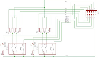
First thing I did was etching a board for two of the encoders because they wouldn't fit well on my prototyping board. I created an eagle library for the part (download) and etched the board which holds the two encoders, two status LED and connects to the mainboard using a 5x2 pin header:

I created the part using the dimensions from the datasheet. It's my first DIY eagle library, so please bear with me if there are some design flaws. It worked fine with my circuit here. Maybe there is some way to make the enclosure pins connect to the GND net. Warning: I used the enclosure as a bridge in my design below.

The schematic. The encoder datasheet contains an application test circuit which shows these resistors with 10k. I also used 10k to drive my PIC portpins.

Below is the board in theory and my toner transfer mask (mirrored!).

I zipped the eagle schematic, board, part library and the etching mask: Download


The finished board, done using Toner transfer and Fe3-Chloride etchant. As you can see, the groundplate is pretty bad. This was my second board ever (after the pic burner board) and this time I heated the toner too few. Also I forgot to mirror the image before printing, so my pin header is different from the schematic. Everything works though ;)


Understanding the encoder output
Second hurdle was to understand how these things output the rotation information. Although there were some examples on the web, I didn't get it until I started from the graph in the datasheet and went tried to write the code for myself. This is the graph from the datasheet:
So, if the two Signal lines are connected to two port pins, I have two bits to read and work with. Only the order of the bit-changes give me the information about turning direction. To see these signals, I connected two LED between each signal line and ground. When turning clockwise, I got 00, then 01, 11, 10, then 00 again. Turning the other way gives 00, 10, 11, 01, 00.
When turning right, the first (right) bit changes after 00 and 11. When turning left, the second (left) bit changes after 00 and 11.
After some trial and error and too many cups of coffee, I had a working code and I was glad having tried it myself. Without this fiddling I'd have never understood the logic behind this.


Testing code
For output, I put the PWM code from last time into a function "void updatepwm(int dutycycle)" and increase or decrease the duty cycle value when turning the knob.
The encoder outputs are connected to RB[0:1].

#include <p18cxxx.h>
#include <p18f2550.h>
#include <delays.h>

//Pin Reset Configurations
#pragma config PBADEN = OFF            //RB0 through RB4 pins are configured as digital I/O on Reset

//Oscillator Settings
#pragma config PWRT = ON               //Soft Power-Up
#pragma config FOSC = HSPLL_HS         //HS oscillator, PLL enabled, HS used by USB 
#pragma config PLLDIV = 5              //PLL prescaler divides by 5 (20 MHz oscillator input) 
#pragma config CPUDIV = OSC1_PLL2      //CPU @PLL/2=48MHz

//Features
#pragma config MCLRE = ON              //MCLR pin enabled; RE3 digital input disabled
#pragma config LVP = OFF               //Single-Supply ICSP disabled, free RB5
#pragma config DEBUG = OFF             //Background debugger disabled, RB6 and RB7 configured as I/O pins
#pragma config WDT = OFF               //HW Disabled - SW Controlled
#pragma config BOR = OFF               //Brown-out Reset disabled in hardware and software
#pragma config STVREN = ON             //Stack overflow/full reset

void init (void);
void main (void);
void updatepwm (int dutycycle);

void main (void)
{
    char laststate = 0;
    char currentstate = 0;
    int brightness = 512;

    init();
    updatepwm(brightness);

    while(1){
        
        //check button on rb2
        if (!(PORTB & 0x04))    //buttonA pulls rb2 to ground
        {
            updatepwm(0);
            brightness = 0;
        } else if (!(PORTB & 0x08))    //buttonB pulls rb3 to ground
        {
            updatepwm(1023);
            brightness = 1023;
        } else
        {
            currentstate = PORTB & 0x03;    //read current encoder input

            //check if encoder input has changed        
            if (currentstate != laststate)
            {    
                //check if first bit changed
                if ((currentstate & 0x01) != (laststate & 0x01))
                {
                    //if both bits were the same before, we're turning right
                    if ((laststate == 0) || (laststate == 3))    //laststate is 00 or 11
                    {
                        brightness = brightness + 16;
                    } else
                    {
                        brightness = brightness - 16;
                    }
                } else {    //second bit changed
                    //now if both bits were the same before, we're turning left
                    if ((laststate == 0) || (laststate == 3))
                    {
                        brightness = brightness - 16;
                    } else
                    {
                        brightness = brightness + 16;
                    }                
                }
            if (brightness < 0) {brightness = 0;}
            if (brightness > 1023) {brightness = 1023;}

            updatepwm(brightness);
            laststate = currentstate;
            }
        }
    }
}

//dutycycle must be a value between 0 and 1023
//see http://h3po-notes.blogspot.com/2009/09/using-hardware-pwm-on-pic18f.html
void updatepwm (int dutycycle)
{
    CCPR1L = dutycycle >> 2;
    CCP1CON = 12 | ((dutycycle << 4) & ~12);
}

void init (void)
{
    //setting up pwm
    TRISC &= ~0x04;        //setup rc2 for ccp1
    CCP1CON = 0x0C;        //0b00XX1100 for single mode pwm
                           //XX are bits [0:1] of the 10bit duty cycle value
    CCPR1L = 0x00;         //reset pwm duty cycle
    PR2 = 0xFF;            //pwm period = 750kHz / 256 ~= 2930Hz
    T2CON = 0x07;          //enable, prescale 1:16 => tmr0 counting at 750kHz

    TRISB |= 0x03;         //rb[0:1] quadrature encoder signals
    INTCON2 |= 0x80;       //disable PORTB pullups
}

Phew.

9/09/2009

Using the Hardware PWM on a PIC18F

Today I tried to use the hardware PWM module of my PIC18F2550 to simply fade an LED. It is easy in the end, but some things confused me on the way:

1) Where to put the duty cycle value?
The name of the configuration register CCPR1L made me think this is the lower 8 bits of the duty cycle value. In fact, these are the upper 8 bits while the lower two bits (=least significant bits, LSB) are bits [5:4] at CCP1CON which also holds the PWM configuration values. This means we always have to split our desired duty cycle value (in my case, an integer counting from 0 to 1023) and write bits [0:1] to [4:5] of CCP1CON and bits [2:9] to [0:7] of CCPR1L. With my limited knowlege of C, this caused a bit of head-scratching here ;)

2) Output Current
When I had my code running, I connected one of my low-current LED to the PWM output with an 1k resistor to ground, which causes the LED to draw about 3.2mA. At this time, I had a small speaker connected to another pin on PORTC (for software PWM) with a small transistor-amplifier. Now each time I used the hardware PWM, this speaker would beep at about my PWM frequency, even though I didn't drive its port pin! Damn, I thought to myself, the PWM causes a lot of noise. Sadly, I don't own an oscilloscope to investigate such problems.
In the end, I set the duty cycle fix to 100% and measured the current drawn on the PWM pin, finding that it would only output 2.9mA max. This means, even my low-current LED overloads the PWM pin. Putting a small signal transistor in between solved things.

Here's my code:
#include <p18cxxx.h>
#include <p18f2550.h>
#include <delays.h>

//Pin Reset Configurations
#pragma config PBADEN = OFF            //RB0 through RB4 pins are configured as digital I/O on Reset
//#pragma config CCP2MX = ON           //CCP2 multiplexed with RC1

//Oscillator Settings
#pragma config PWRT = ON               //Soft Power-Up
#pragma config FOSC = HSPLL_HS         //HS oscillator, PLL enabled, HS used by USB 
#pragma config PLLDIV = 5              //PLL prescaler divides by 5 (20 MHz oscillator input) 
#pragma config CPUDIV = OSC1_PLL2      //CPU @PLL/2=48MHz

//Features
#pragma config MCLRE = ON             //MCLR pin enabled; RE3 digital input disabled
#pragma config LVP = OFF              //Single-Supply ICSP disabled, free RB5
#pragma config DEBUG = OFF            //Background debugger disabled, RB6 and RB7 configured as I/O pins
#pragma config WDT = OFF              //HW Disabled - SW Controlled
#pragma config BOR = OFF              //Brown-out Reset disabled in hardware and software

void main (void);

void main (void)
{ 
    
    TRISC &= ~0x04;    //clear rc2 tris bit for output

    CCP1CON = 0x0C;    //0b00XX1100 for single mode pwm
                       //XX are bits [0:1] of the 10bit duty cycle value
    CCPR1L = 0x00;     //reset pwm duty cycle bits [2:9]
    PR2 = 0xFF;        //pwm period = 750kHz / 256 ~= 2930Hz
    T2CON = 0x07;      //enable, prescale 1:16 => tmr0 counting at 750kHz
    
    while(1){
        //fade from 0 to 5v
        for (i = 0; i < 1024; i++)
        {
            CCPR1L = i >> 2;                     //shifting bits [2:9] to [0:7]
            CCP1CON = 12 | ((i << 4) & ~12);     //clearing bits [2:3]
                                                 //shifting bits [0:3] to [4:7]
                                                 //and setting bits [2:3] for pwm configuration
            Delay10KTCYx(5);
        }
        
        //fade back to 0v
        for (i = 1023; i >= 0; i--)
        {
            CCPR1L = i >> 2;
            CCP1CON = 12 | ((i << 4) & ~12);
            Delay10KTCYx(5);
        }
    }
}
Testing Circuit
The Transistor is a BC338 with a hfe of ~400, so when drawing 3.1mA for the LED, the pwm output pin only has to deliver 1/400th of this current.

9/04/2009

Late introduction post

I just have the feeling I should write some kind of introduction post and give some information about who I am and what I do. So here it is:
  • You can find me everywhere by the nick H3PO.
  • I've just finished school and don't have any electronics degree or something, so don't expect pure wisdom and ingeniuity here. I'm just fiddling until things work as I like it.
  • Until now, I just used to program things in VB6, which is slowly disappearing. I have to use an XP virtual machine to run the IDE.
  • As you can see, I'm programming for Windows. I try switching to linux every once in a while, but currently Win7 RC satisfies all my needs.
  • I like bullet lists :P
So what is it with this PIC stuff?
I recently built a remote-shutter and timer for my digital camera using the old NE555, the performance was disappointing (20mA consumtion for switching a transistor every 3-180s...) and I felt the need for some refreshing digital stuff. This is when I thought about learning to program a µC.
After reading some comparisons between AVR and PIC, I had the feeling it just wouldn't matter in the beginning, but possibly be a problem in the past choosing the "wrong" platform to learn. In the end, I voted for the PIC because I knew someone with an LPT PIC programmer and some experience.
I had a pretty hard start because I didn't have a parallel port and couldn't get my serial port to talk. I didn't want to buy something either, so I decided to build an USB based programmer according to a design found on sprut.de (German). The programmer itself is powered by a PIC, so I needed a kick-start from my friend who was so kind to burn the programmer firmware to my first PIC18F2550.

The circumstances my future projects are based on:
  • My burner is the Brenner8mini-P from sprut.de suitable for all 5V models with 11-13V programming voltage
  • I'm using the free version of the Microchip C18 Compiler and MPLAB. I haven't had any experiences with any kind of C yet.
  • On most of my breadboard photos, you'll see my ICSP connection to the burner with orange being DATA, brown CLOCK and yellow Vpp
  • Before trying my first programs, I read the datasheet and some information about incorporating an ICSP header into a circuit. In the end, I came up with this basis breadboard which enables my burner to power the pic for the time of programming:


So far. Enjoy yourselves building things. Please leave comments if you like what I post and share your thoughts on corrections and improvements.

8/29/2009

Using the DAC on a PIC18F2*550

I tried to figure out how to use the integrated DAC. I have a 2k7 Potentiometer (unfortunately, a non-linear one) connected between Vdd and Vss, the terminal goes to AN0. AN1:AN6 drive 6 LED to form a simple bar-graph display showing the captured voltage.

#include <p18cxxx.h>
#include <delays.h>

#pragma config MCLRE = ON      //MCLR pin enabled; RE3 digital input disabled
#pragma config WDT = OFF       //HW Disabled - SW Controlled
#pragma config BOR = OFF       //Brown-out Reset disabled in hardware and software 

#pragma config FOSC = INTOSCIO_EC     //Internal oscillator, port function on RA6, EC used by USB 
#pragma config LVP = OFF              //Single-Supply ICSP disabled, free RB5
#pragma config PBADEN = OFF           //RB0 through RB4 pins are configured as digital I/O on Reset
#pragma config DEBUG = OFF            //Background debugger disabled, RB6 and RB7 configured as I/O pins

void init (void);
void main (void);

void init (void)
{
    OSCCON = 0xFF;    //internal oscillator at 8MHz
                      //1ms = 2000000 Instructions

    ADCON0 = 0x01;    //Enable ADC on Channel AN0
    ADCON1 = 0x0E;    //ADC on AN0, VDD and VSS reference
    ADCON2 = 0xA7;    //Right justified, 8TAD, FRC Clock
}

void main (void)
{

    int adc;

    init();
    TRISA = 0x00;
    LATA = 0x7E;    //1st bit used by ADC, last bit non existent

    while (1)
    {
        ADCON0bits.GO_DONE = 1;            //Start the DAC
        while (ADCON0bits.GO_DONE) {}      //Wait for the DAC to finish calculating
        adc = ADRESL + (ADRESH * 256);     //Add the two 8-bit registers into one Integer
        //LATA = (adc / 16) << 1;          //for testing, you can output the value
                                           //in binary

        if (adc  >= 876)                   //6 LED + Off = 7 states
        {LATA = 0x7E;}                     //adc >= 6/7*1023, adc >= 5/7*1023 and so on.
        else if (adc  >= 730)
        {LATA = 0x3E;}                     //Light 6 LED
        else if (adc  >= 584)
        {LATA = 0x1E;}                     //Light 5 LED
        else if (adc  >= 438)
        {LATA = 0x0E;}                     //...
        else if (adc  >= 292)
        {LATA = 0x06;}
        else if (adc  >= 146)
        {LATA = 0x02;}
        else
        {LATA = 0x00;}
          
        Delay10KTCYx(1);    //According to the datasheet, we only have to wait
                            //4 instructions after collecting data
     }
}

Test circuit:

8/26/2009

Get all possible digital inputs on a PIC18F2*50

Same thing as last post, the other way round.

Pins available for digital input:

  • PORTA: RA0 through RA6 gives 7 inputs
  • PORTB: RB0 through RB7 gives 8 inputs
  • PORTC: RB0 through RB2 and RB4 through RB7 gives 7 inputs
  • PORTE: RE3 gives one input
=> on a PIC18F2*50 you have 23 digital outputs total.

Configure options:
  • FOSC = INTOSCIO_EC //using the internal oscillator will free pins RA5 and RA6
  • LVP = OFF //you don't have to ground RB5 anymore
  • PBADEN = OFF //disable the analog inputs on RB0 through RB4
  • DEBUG = OFF //disable debug output, free RB6 and RB7
  • MCLRE = OFF //disable the master clear option, free RE3

Registers to set:
  • ADCON1 = 0x0F; //disable analog inputs on RA0 through RA3
  • UCON = 0x00; //disable the usb module, free RC4 and RC5
  • UCFG = 0x08;
RC4, RC5 & RE3 can only be used as digital inputs, not as outputs. PORTB has internal pullups which can be activated by clearing bit7 at INTCON2. This is very handy for me because I have wildly fluctuating inputs here with the breadboard and power over my pc's USB.

Get all possible digital outputs on a PIC18F2*50

Recently I've been experimenting with a PIC18F2550 microcontroller and it wasn't easy at all to get the ports running in the mode I wanted to. So at first, I looked through the datasheet to find out which ports can be used as digital output pins and how to configure them. This is what I came up with:

Available output pins:
  • PORTA: RA0 through RA6 gives 7 outputs
  • PORTB: RB0 through RA7 gives 8 outputs
  • PORTC: RC0 through RC2, RC6 & RC7 gives 5 outputs
=> on a PIC18F2*50 you have 20 digital outputs total.

Configure options:

  • FOSC = INTOSCIO_EC //using the internal oscillator will free pins RA5 and RA6
  • LVP = OFF //you don't have to ground RB5 anymore
  • PBADEN = OFF //disable the analog inputs on RB0 through RB4
  • DEBUG = OFF //disable debug output, free RB6 and RB7
    Registers to set:
    • ADCON1 = 0x0F; //disable analog inputs on RA0 through RA3

    One comment on using RB6 & RB7: You'll have to interface these pins over at least 10k resistors to be able to do ICSP programming on these pins. If you can avoid it, don't use these pins for I/O in your circuit.

    Testing code:
    #include <p18cxxx.h>
    
    #pragma config MCLRE = ON             //MCLR pin enabled; RE3 digital input disabled
    #pragma config WDT = OFF              //HW Disabled - SW Controlled
    #pragma config BOR = OFF              //Brown-out Reset disabled in hardware and software
    
    #pragma config FOSC = INTOSCIO_EC     //Internal oscillator, port function on RA6, EC used by USB
    #pragma config LVP = OFF              //Single-Supply ICSP disabled, free RB5
    #pragma config PBADEN = OFF           //RB0 through RB4 pins are configured as digital I/O on reset
    #pragma config DEBUG = OFF            //Background debugger disabled, RB6 and RB7 configured as I/O pins on reset
    
    void main ( void );
    void init ( void );
    
    void init (void)
    {
        OSCCON = 0xFF;    //8MHz internal clock
                          //1ms = 2000000 Instructions
        ADCON1 = 0x0F;    //Set multiplexed pins on PORTA to digital
        TRISA = 0x00;     //Configure RA0 through RA6 as output
        TRISB = 0x00;     //Configure PORTB as output
        TRISC = 0x00;     //Configure RC0:RC3, RC6:RC7 as output
        LATA = 0x00;      //Reset Pins
        LATB = 0x00;
        LATC = 0x00;
    }
    
    void main (void)
    {
        init();
    
        LATA = 0x7F;     //01111111
        LATB = 0x3F;     //00111111
        LATC = 0xC7;     //11000111
    
        while (1) {}
    }
    Result

    My PIC18F2550 controlling 18 low-current (!) LED independently. RC6 and RC7 were needed for ICSP.
    The maximum rated current per Pin is 20mA, Vss (Ground) can only handle 200mA. Caution: Using standard LED would fry the ports!